The Golden Age of Ever-Changing Computer Architecture
Given the accuracy of Moore’s Law to the development of integrated circuits over the years, one would think that our present day period is no different from the past decades in terms of computer architecture design. However, during the 2017 ACM Turing Award acceptance speech, John L. Hennessy and David A. Patterson described the present as the “golden age of computer architecture”.
Compared to the early days of MS-DOS, when designing user- and kernel-space interactions was still an experiment in the works, it certainly feels like we’re no longer in the infancy of the field. Yet, as the pressure mounts for companies to acquire more computational resources for running expensive machine learning algorithms on massive swaths of data, smart computer architecture design may be just what the industry needs.
Moore’s law predicts the doubling of transistors in an IC, it doesn’t predict the path that IC design will take. When that observation was made in 1965 it was difficult or even impossible to envision where we are today, with tools and processes so closely linked and widely available that the way we conceive processor design is itself multiplying.
Once Stratospheric Development Costs Have Become Merely Sky-High
In the past, innovation in computer architecture could be a risky move for a business to undergo, especially if there wasn’t any good reason why the industry standard had to be surpassed. At best, they could spend a fortune investing in R&D and output a game-changing design. At worst, they could tank their company and end up with a massive stock of unsellable units. While ideas like increasing cache sizes or buffer sizes could optimize one chokehold of an architecture, either the logistics of manufacturing or the costs of production can surpass these re-adjusted sticking points. Prior to VLSI, it would have been incredibly difficult to include as many processes on a single chip, and long wires between large components slowed down computation.
It is inarguable that with the democratized chip design by Mead and Conway and developments like RISC architecture, branch prediction, and the high-level programming languages that use them, the 1980s ushered in major innovations for computer architecture. It begs the question, where is the peak? Dennard scaling (a scaling law that states that as transistors get smaller, their power density stays the same, resulting in significant frequency increases) may have ended in 2006, and Moore’s Law looks to be breaking down in the near future, but with major industry support for faster computation in machine learning, and renewed interest in higher-level languages, domain specific architectures and custom-manufactured chips seems to be ushering in innovation for a different view of computer architecture. A focus on supercomputers and niche chips may help improve computation even faster than Moore’s Law predicts.
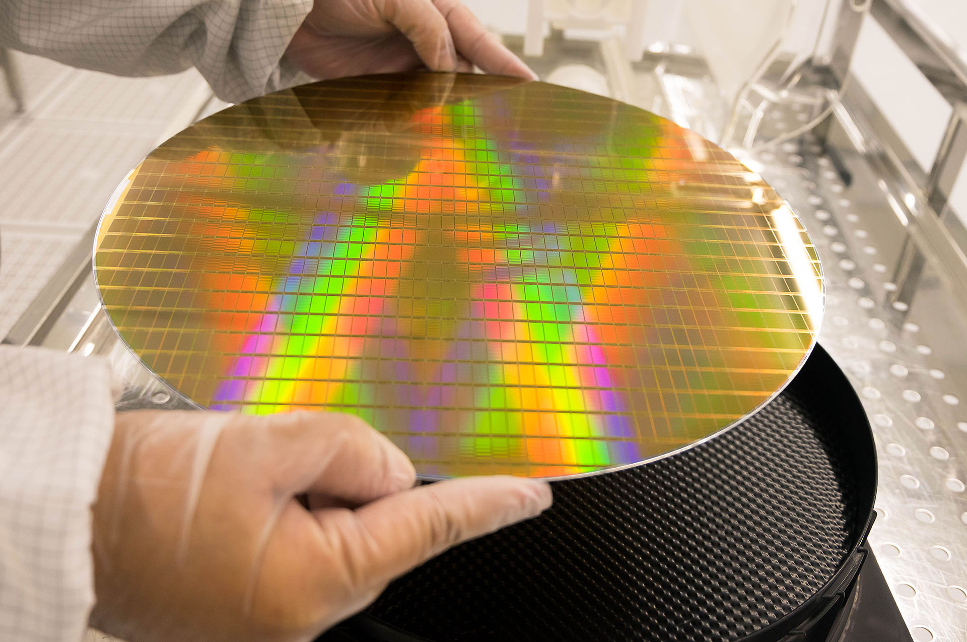
Uncorking the Bottleneck of Silicon Production
The new wave of Chinese semiconductor manufacturing is no secret — in 2014, The State Council of China issued the National Guidelines for Development and Promotion of the Integrated Circuit (IC) Industry, a national policy for improving the country’s semiconductor production. They increased investment, adopted a market-based approach, and focused on creating national champions through changes in industry revenue generation, production volume, and technological advances. With surging demand for Chinese smartphones (Huawei, Lenovo, Meizu, Xiaomi) and China-based consumer demand, there has been a lot of encouragement for improving manufacturing throughput.
While Chinese chip manufacturers may not be producing the most advanced architectural designs, they are still edging out competition in terms of the affordability and efficiency of their processes. Funding for nanoscience, cheap labor, and lower costs for factory maintenance and materials all contribute towards the lower cost of Chinese products, although there are also other manufacturers in countries such as Taiwan and Vietnam that are similarly providing cheap fabrication services.
To see how far silicon production has come it’s interesting to look at Application-Specific Integrated Circuits (ASICs) — chips designed to perform a particular set of operations better (in terms like power or speed) than a general CPU could.
In the 1980’s the manufacturing of ASICs was a process that required a separate designer and manufacturer since there wasn’t a direct link between third-party design tools and semiconductor processes. Since then the process for manufacturing custom chips has massively improved. The results are obvious. For instance, the popularity of Bitcoin mining drove many new ASIC designs, as specialty hardware would provide greater hash power at a lower price, which translates into greater profits from electricity. Companies like Halong Mining, Bitmain, and BitFury produced — and continue to sell — a flurry of mining hardware to Bitcoin hopefuls. Many realized that the capabilities of GPUs to process large amounts of visual data efficiently was closely tied to the resource needs of new algorithms, ASICs can do the same but at a lower cost and power budget. You can probably guess that the algorithms now driving the industry focus on machine learning.
Architectures for Machine Learning
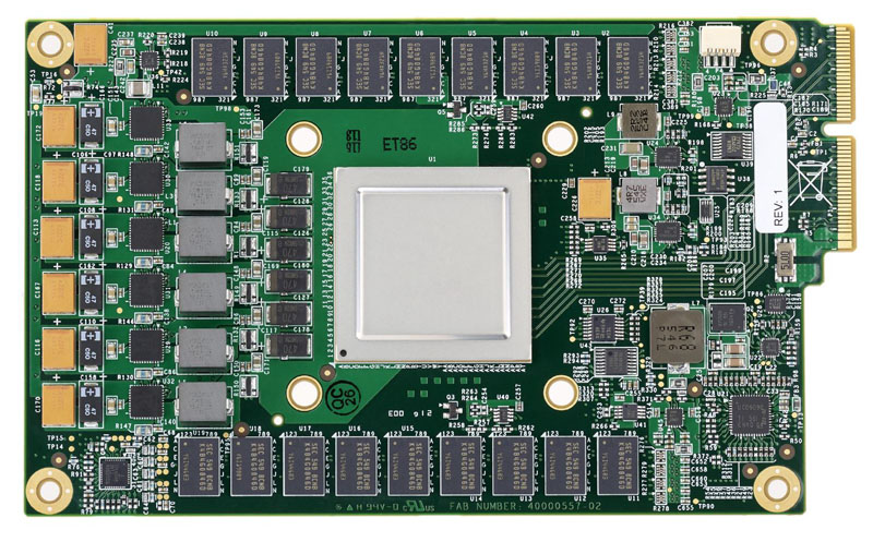
In 2016, Google announced their commercial TPU, one of the first chips created specifically for the purpose of running machine learning algorithms. TPUs are used within the company for neural network computations behind products such as Google Search, Street View, Google Photos and Google Translate. Compared to RISC architecture, which focuses on simpler instructions that are used for a larger portion of applications (load, store, add, multiply), the TPU is based on CISC (Complex Instruction Set Computer) architecture, which implements higher-level instructions for running more complex tasks (such as many multiplies and adds for matrix multiplication).
Some other differences that mark the TPU as an improvement over CPUs and GPUS are the systolic array, deterministic design, and quantization choices. The systolic array mimics how the heart pumps blood since data flows through the chip in waves. For matrix multiplication, this is especially useful since the same inputs are reused many times without being stored back to a register. Wires only connect adjacent ALUs that performed fixed patterns of multiplication and addition, simplifying their design and shortening the wires needed.
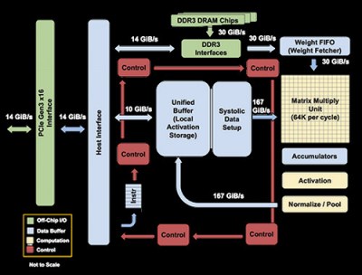
Deterministic design seeks to be ultimately minimal, with no requirement for supporting a wider range of applications than neural network models. Due to the nature of the chips, prediction is much more reliable since only neural network predictions are ever being run. Control is a lot easier to design than for CPUs and GPUs, and while more ALUs and on-chip memory are needed for TPUs, they tend to be smaller than other chips. This has the nice side effect of reducing cost (a function of area cubed) and increasing yield since smaller chips are less likely to have manufacturing defects.
Quantization uses an 8-bit integer for approximating a value given a max and min value. The technique helps reduce noise in calculations, since neural network predictions don’t require floating point precision with 32-bit or 16-bit values. Even an 8-bit value can suffice for the levels of accuracy needed, thus reducing the size of models quite dramatically.
There is also the matter of flexibility. Because the TPU is programmable, it is able to accelerate computations for many different types of neural network models. The computational resources used include a Matrix Multiplier Unit (MXU), Unified Buffer (UB) or SRAM working as registers, and an Activation Unit (AU) for hardwired activation functions. A dozen high-level instructions interface with these resources, such as multiplying or convolving with data and weights, reading weights from memory, and applying activation functions.
Microchips No Longer All That Micro
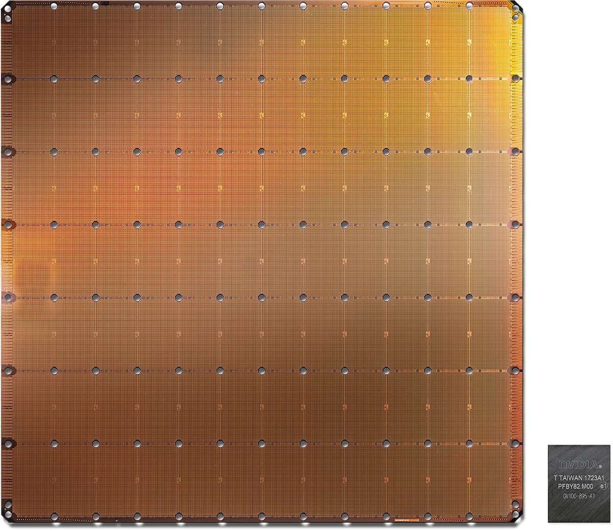
One of the most viral stealth companies, Cerebras, has been working on the largest silicon chip ever built. It measures at 46,225 mm2 of silicon, with 1.2 trillion transistors. Compared to the largest GPU, it’s nearly 100x the size. The chip is designed around handling tensor operations and moving around data more efficiently. With SRAM memory on the chip, it simplifies operations that would typically travel longer distances within a cluster to processes that can communicate on the same chip. While there are general operations supported for control processing, there are also optimized tensor operations for data processing. In terms of the materials inefficiencies involved with the high power consumption and heat generation, a connector layer between the silicon and PCB handle the mechanical stress created by thermal expansion while a cold plate transfers away heat from the wafer chip.
The chip boasts 1.2 trillion transistors, 400,000 AI optimized cores, 18 Gb on-chip memory, and 9 PB/s of memory bandwidth. Compared to the Nvidia GeForce RTX 2080 Ti GPU, with 18.2 billion transistors, 4,352 CUDA cores, 11 Gb on-chip memory, and 616 GB/s of memory bandwidth, it is clear that the Cerebras has massive improvements over even the best commercially available GPUs. What had once been a manufacturing nightmare has become a reality with improvements in silicon manufacturing.
An Ever-Changing Landscape
With Moore’s law constantly on the horizon, researchers are constantly on the lookout for new methods for reducing latency in computation. Concepts such as neuromorphic computing, probabilistic computing, and quantum chips are making their way from theory to development. Neuromorphic computing uses low-power artificial synapses to mimic the neural structure of the human brain, although matching human cognitive flexibility can be challenging. Quantum chips have an immense number of factors that must be controlled in order to maintain the integrity of the qubits — the quantum bits most commonly created by a Josephson junction (superconductors coupled by a weak link consisting of a thin insulating barrier).
Just as Dennard may not have been able to foresee multicore processors, Moore was likely unable to predict the advent of machine learning and its effect on hardware manufacturing. Even the most creative visions for the future of computer architecture will have a difficult time predicting just how far computing will go, and to what lengths new companies will take memory and instruction set manipulation to strive for ever-increasing speed in the coming decade.
from Hackaday https://ift.tt/2XT5z70
Comments
Post a Comment